Researcher Spotlight
Nanofabrication at the molecular scale - MIT-Harvard Center for Excitonics
It is possible to write one nanometer structures. Such a structure is only five atoms wide and, to make this more challenging, we would like to be able to do this in a matter of microseconds. Does this sound a bit like a sci fi fantasy? In fact, it refers to current technology being developed to enable working with the tiniest possible specimens, in this case, quantum dots (QDs). The accurate manipulation of QDs, which can confine excitons within a nano scale ‘dot’, will help us to develop circuits for excitons and more efficiently convert photons from the invisible part of the solar radiation spectrum. Even so, the fanciest recent high tech methods often have roots in something very traditional.
Graduate student Vitor Manfrinato hopes that he can lay important groundwork toward this goal by using electron beam lithography (EBL). EBL is analogous to methods used in printing presses, and in the conventional fabrication of electronic devices. Lithography transfers a pattern from a master to a copy. A printing press is a form of lithography and traditionally uses a stamp to transfer ink onto paper. Optical lithography is currently used by the electronics industry to define high resolution features within computer chips. This process uses an opaque patterned mask to shine light on only selected regions of a silicon wafer. Then chemical processes are used to transfer this information into structures on the wafer. Vitor and his collaborators seek a new alternative that offers even smaller features without incurring impractical costs. Vitor’s research process involves using beams of electrons to define patterns on a smaller scale than even optical lithography can. He is changing the materials and techniques to find ways to improve production efficiency at the scale of individual atoms.
To better understand the problem at the atomic scale, we must begin at the beginning, with the idea of nanofabrication – making very small things. In the mid-1990s, the smallest structure (or pattern) ever created1 was made by Don Eigler and Erhard Schweizer at IBM Almaden, when they spelled “IBM” with xenon atoms on nickel substrate. They used a scanning tunneling microscope to manipulate those atoms. That was an important milestone in the field of nanotechnology, as it set the resolution limit for lithography. However, a downside of their technique is that it was extremely slow and complex to execute – making the “IBM” took a whole day – so it is not currently used for nanomanufacturing.
An integrated effort
Vitor’s work is supported by expertise within the Center for Excitonics and his work will help advance work in other groups within the Center. He is a member of the Quantum Nanostructures and Nanofabrication Group led by Prof. Karl Berggren, and works closely with Moungi Bawendi’s Semi-Conductor and NanoCrystal’s group, which pioneered the synthesis and the physics of QDs.
He also collaborates with Brookhaven National Laboratory principal investigator, Eric Stach, on the large scanning transmission electron microscope (STEM) that resides there. The Brookhaven National Laboratory in New York is a federally funded energy laboratory and is the Center’s partner institution. Vitor and collaborators use the ultra-high resolution STEM to fabricate the few-atom structures. Dr. Stach’s group at Brookhaven, the Center for Functional Nanomaterials (CFN), employs the STEM on an on-going basis to look for new properties and materials at the nanoscale to make energy harvesting devices.
Using this technique, Vitor hopes to continually improve his ability to control the position of QDs in exactly the spots he wants. Eventually, he along with others can then try to engineer the transfer of energy between them, leading to new opportunities in solar devices. To date, using electron-beam lithography (EBL) has enabled the creation of structures down to 9 nm pitch (i.e., 9 nm periodic dense patterns). As we know, Vitor has been aiming for smaller. He selected the material HSQ – hydrogen silsesquioxane – because Prof. Karl Berggren’s team has previously demonstrated that very high resolutions were possible with this material. So, after exposing the HSQ substrate at Brookhaven, Vitor brings the materials back to MIT for further analysis. In 2011 Vitor and his team successfully demonstrated improvement of patterning speed with low-energy electrons2 and with neon ions;3 this last technique was 1,000 times more efficient than EBL. They conclude that these techniques are promising for fast and energy-efficient nanomanufacturing.4
A passion for engineering
Vitor, a Brazilian by birth and a third-year graduate student in RLE’s Center for Excitonics, is a scientist with an entrepreneurial spirit.
He has a vision: he strongly feels it is possible to develop faster and more cost-effective manufacturing processes and he is in part driven by the knowledge this could help society.
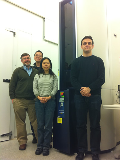
(from left to right) Eric Stach, Dong Su, Lihua Zhang, Vitor Manfrinato at Brookhaven National Laboratory with STEM microscope
He is also motivated by a deep fascination with the natural world. He says that his work, in a real sense, attempts to recreate nature’s building blocks in trying to understand how energy is channeled through natural systems. He expects to produce some new ways to control light and energy transfer and this will someday lead to more cost-effective sources of lighting.
So how did Vitor choose his path? He has considered himself as an inventor from the moment he picked up his first set of Legos™. As a high school student, he was happy to discover that invention was what the field of engineering is all about; he realized if he pursued studies in electrical engineering, he would learn about the tools and background he needed. He was so drawn to research that he emailed two professors at MIT, and he came to MIT when he was 23 to spend a semester working on a project with Professor Jing Kong. This work became his senior thesis. Vitor says, “(In engineering) you want to break down a complicated problem into its smallest unit and understand its inputs and outputs, and then put them together with other tools.” Thus, the combination of great ideas with creative engineering design work by Vitor and many of his colleagues within the Center for Excitonics has the potential to impact the future of nanomanufacturing and society’s need for more efficient and effective light harvesting devices.
Portuguese Translation (Para Tradução Português)
1 “35 atoms that changed the nanoworld” Nature Nanotechnology, Vol. 5, April 2010.
2 Vitor R. Manfrinato, Lin Lee Cheong, Huigao Duan, Donald Winston, Henry I. Smith, Karl K. Berggren “Sub-5 keV Electron-Beam Lithography in Hydrogen Silsesquioxane Resist,”, Microelectronic Engineering 88
(2011) 3070-3074.
3 Donald Winson, Vitor R. Manfrinato, Samuel M. Nicaise, Lin Lee Cheong, Huigao Duan, David Ferranti, Jeff Marshman, Shawn McVey, Lewis Stern, John Notte and Karl K. Berggren, “Neon Ion Beam Lithography,”NanoLetters, 2011, 11 (10), pp 4343–4347.
4 See “The future of chip manufacturing” – http://web.mit.edu/newsoffice/2011/future-chips-0630.html?tmpl=component&print=1